pulse
qendra pulse delivers high-fidelity RF waveform control with nanosecond-level precision. Developed for trapped-ion and neutral-atom experiments, pulse generates synchronized signals for every stage — from cooling to measurement.
The AMD ZCU216 ready for AOM control
Integrated intensity stabilization can be as simple as pie
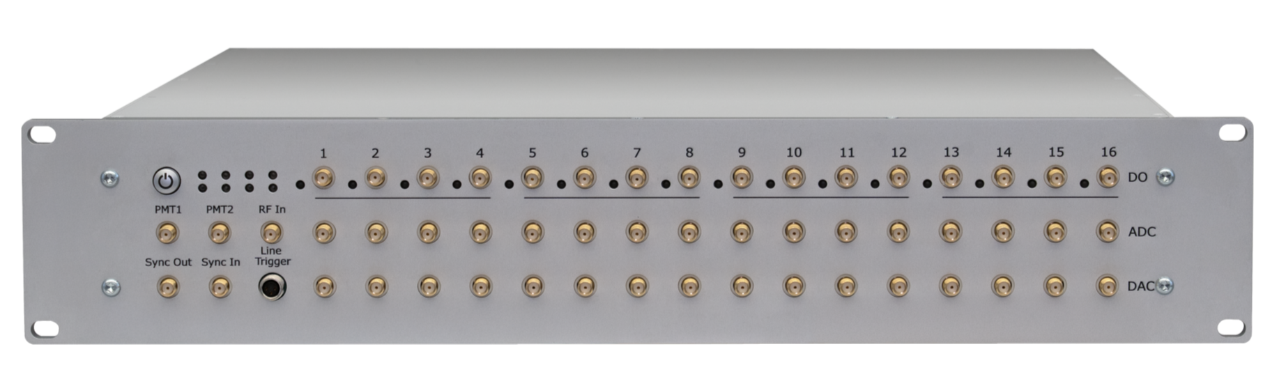
16 RF outputs, 16 ADC channels, 16 digital outputs. Ready to pulse
RF outputs
| Property | Quantity |
|---|---|
| Channels | 16 |
| Skew | Length matched in groups of 4, 0.7 ns between earliest and latest group |
| Sampling rate | 1 GSPS |
| Frequency resolution | 32 bits (0.23 Hz) |
| Amplitude resolution | 14 bits (84 dBFS) |
| Phase resolution | 16 bits (96 μrad) |
| Time resolution | 4 ns |
| Minimum pulse time | 40 ns |
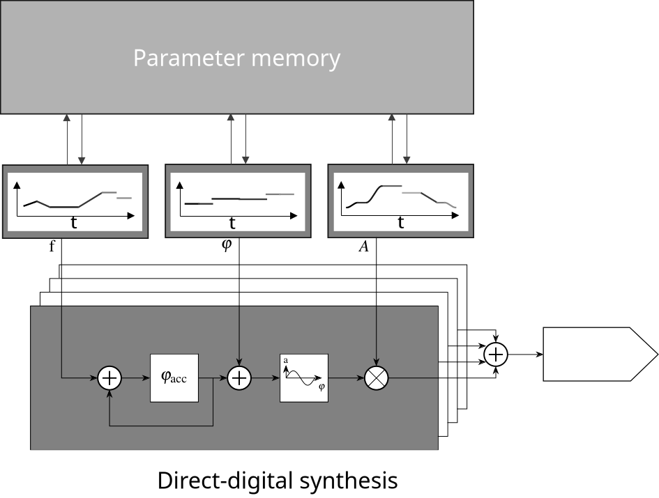
| Digital waveform generation | 4 sinusoids per physical channel |
| Frequency modulation | Linear interpolation |
| Amplitude modulation | Cubic polynomials |
| Phase modulation | Zero-order hold |
| Parameter storage per channel | 1 Mib (5957 cubic polynomials or 10922 linear segments) |
| Sequence storage per channel | 640 Kib (20480 instructions or 2560 unique pulses) |
| Waveform memory per channel octet | 1 GSa |
| AWG channels per channel octet | 3 (triggered simultaneously, can be output on any of the 8 channels of the octet) |
| NCOs per channel | 4 |
| Output frequency | 0.2 – 450 MHz (AC coupled) |
| Output power | 5 dBm |
| Phase noise | -139 dBc/Hz @ 10 kHz -148 dBc/Hz @ 1 MHz |
The numerically controlled oscillators (NCOs) operate in phase-coherent switching mode by default. The output phase is referenced to the beginning of the pulse sequence.
To meet the demands of neutral atom quantum experiments, the frequency modulator will receive an optional upgrade to support cubic polynomials (tentatively scheduled for Q2 2026). Additionally, the channel mapping will be customizable with multiple logical channels added together to a single physical output or the individual NCOs per channel fanned out to multiple physical channels (e.g. physical channel RF 0 outputs the sum of logical channel CH 0, 1, 2 and 3, while frequency tone 0 and 1 of CH 4 are routed to RF 1 and tone 2 and 3 are routed to RF 2). The multi-channel mapping feature is scheduled for Q2 2026 as well.
Analog inputs
| Property | Quantity |
|---|---|
| Channels | 16 |
| Skew | 1.3 ns between earliest and latest channel |
| Sampling rate | 62.5 MSPS |
| Amplitude resolution | 14 bits (84 dBFS) |
| Time resolution | 16 ns |
| Input frequency | 0 - 8 MHz (DC coupled) |
| Voltage range | ± 0.5 V |
| Input termination | 50 Ohms, differential (isolated ground) |
| Modes | Photodiode monitoring and integrated intensity stabilization |
Digital outputs
| Property | Quantity |
|---|---|
| Channels | 16 |
| Voltage level | 5 V |
| Galvanic isolation | Isolated from chassis and from each other in groups of 4 |
| Time resolution | 4 ns |
| Minimum pulse time | 12 ns |
| Sequence storage | 1 Mib (32768 instructions or 8192 unique pulses) |
Digital inputs
| Property | Quantity |
|---|---|
| Channels | 3 (including 1 AC-coupled input for < 300 MHz signals) |
| Voltage level | 5 V |
| Time resolution | 4 ns |
| Modes | Time tagging and gated counting |
| Counter width | 18 bits |
| Maximum window length | 4 minutes |
| Line trigger | Included |
Sequencer
Advanced sequencing capabilities support loops, branching and functions. A sequence of pulses can be repeated up to 16.7 million times and called at multiple different times of the same experimental sequence. Loops and functions can be nested up to a total of 8 levels. An efficient use of these features makes it possible to efficiently reuse sequence blocks such as sideband cooling or syndrome measurement.
This functionality is complemented with real-time parameter and sequence updates that are popped from a queue in real time. This makes it possible to scan the length and parameters of a pulse within a loop. Furthermore, this can be combined with branching to completely change the sequence structure between loop iterations.
Readout processing
QuENCH follows a CPU-FPGA-hybrid architecture. While the pulse generation and sequencing are offloaded completely to dedicated sequencers on the FPGA, the CPU remains responsible for analysing the readout results. This is possible with atom-based quantum computing because the typical times of a readout operations are much longer than 100 μs such that latencies up to multiple μs are acceptable.
This simplifies the implementation of mathematically non-trivial schemes such as adaptive maximum likelihood readout. Using the branching functionality of the sequencers, the CPU can efficiently steer the further flow of the sequence by updating few instructions in the instruction memory.
This way, latencies of 2 μs were achieved using older hardware based on the AMD Zynq-7020 SoC.